Wafer-scale, flexible thin-film electronics
January 14, 2014

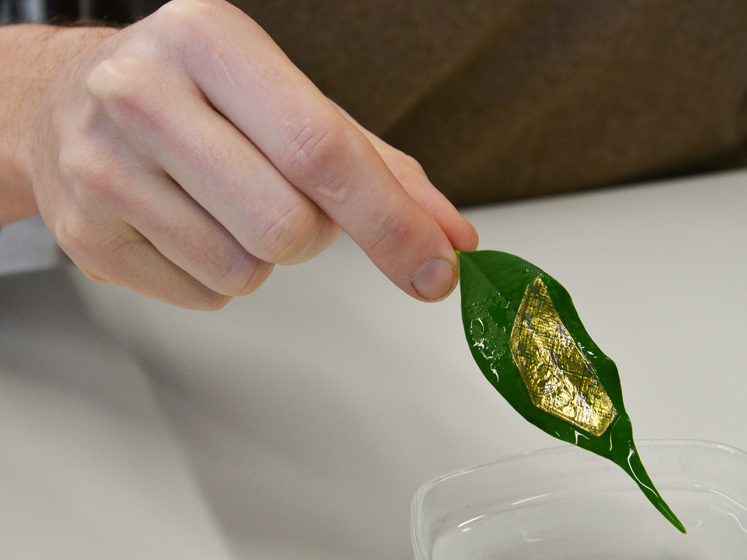
Metallic thin film sticks to leaf (credit: Peter Rüegg/ETH Zürich)
Researchers at ETH Zurich are developing thin-film transistors, sensors, and other electronic components that are thin and flexible enough to be wrapped around a wide range of surfaces without damaging the electronics.
The aim is to weave these types of components into textiles or apply them to the skin to make “smart,” unobtrusive, comfortable sensors that can monitor various functions of the body, aka “temporary tattoo” biosensors.
Electronic components fabricated with this process are extremely flexible, adaptable and — depending on the material used for the transistors — can also be transparent, the researchers say.
How to fabricate flexible thin-film electronics

The proposed engineered substrate consists of two soluble films (PVA and PVAc) and a non-soluble layer (parylene) deposited on a rigid or flexible support. The selective dissolution of the layers enables removal of the support. The proposed process scheme can be implemented at wafer scale, tested here with a 2-inch wafer. (Credit: ETH Zurich)
1. Create a membrane by evaporating the polymer parylene layer by layer onto a conventional two-inch wafer. The parylene film has a maximum thickness of 0.001 mm (1 micron), making it 50 times thinner than a human hair.
2. Using conventional methods, build transistors and sensors from semiconductor materials, such as indium gallium zinc oxide, and conductors, such as gold.
3. Release the parylene film with its attached electronic components from the wafer.
The researchers confirmed the theoretically determined bending radius of 50 microns during experiments in which they placed the electronic membrane on a human hair and found that the membrane wrapped itself around the hair with perfect conformability. The transistors, which are less flexible than the substrate due to the ceramic materials used in their construction, still worked perfectly despite the strong bend.

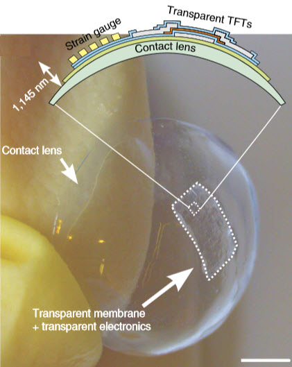
Transparent, light electronics for smart contact lens, affixed to a plastic contact lens held between two fingers (scale bar, 2.5 mm) (credit: ETH Zurich)
“There are organic transistors that can be bent to even smaller radii, but here we used oxidic materials, which provide much better electrical performance,” ETH researcher Niko Münzenrieder told KurzweilAI. “So we think this technology represents a good trade off between flexibility and performance.
“At the moment, we are still in a research phase, but the goal is to integrate electronic functionality, like sensors, into everyday objects, so the technology could be used to fabricate wearables, e.g., for sports, that monitor physiological parameters like body temperature.”
“Smart” contact lenses
One application of this method is “smart” contact lenses. In the initial tests, the researchers attached thin-film transistors, along with strain gauges, to standard contact lenses.
They placed these on an artificial eye and were able to examine whether the membrane, and particularly the electronics, could withstand the bending radius of the eye and continue to function.
The tests showed that the smart contact lens could be used to measure intraocular pressure, a key risk factor in the development of glaucoma.
Abstract of Nature Communications paper
Electronics on very thin substrates have shown remarkable bendability, conformability and lightness, which are important attributes for biological tissues sensing, wearable or implantable devices. Here we propose a wafer-scale process scheme to realize ultra flexible, lightweight and transparent electronics on top of a 1-μm thick parylene film that is released from the carrier substrate after the dissolution in water of a polyvinyl-alcohol layer. The thin substrate ensures extreme flexibility, which is demonstrated by transistors that continue to work when wrapped around human hairs. In parallel, the use of amorphous oxide semiconductor and high-K dielectric enables the realization of analogue amplifiers operating at 12 V and above 1 MHz. Electronics can be transferred on any object, surface and on biological tissues like human skin and plant leaves. We foresee a potential application as smart contact lenses, covered with light, transparent and flexible devices, which could serve to monitor intraocular pressure for glaucoma disease.